Step 1: Calculate Ipad and Vcore:
| Ipad = |
|
| = |
0.9⁄(1.2×16) = 0.047A |
| Vcore = |
| Vddmin(1−2× |
Ipad |
×(Rpkg+Rbond+Rpad)) |
| |
Vdd |
|
|
| = |
1.17×(1−2×0.047×(0.022+0.02+0.04)⁄1.2 |
| = |
1.163V |
Step 2: Calculate the reference power
supply conductance G:
| G = |
|
|
| = |
7 ⁄ (4 × 0.06) = |
29.17 mhos |
Step 3 is to set out the values of
kan, kwn, kcn and mn
for each metal layer, and use these to calculate the value of L.
| metal layer |
1 |
2 |
3 |
4 |
5 |
6 |
| kan |
100% |
100% |
100% |
100% |
180% |
200% |
| power metal allocated coefficient |
| kwn |
70% |
80% |
92.5% |
80% |
132.5% |
135% |
| power metal used coefficient |
| kcn |
75%¹ |
100% |
100% |
100% |
100% |
300%² |
| conductivity coefficient |
| mn |
50% |
50% |
50% |
50% |
50% |
0% |
| core area blocked |
|
| ¹75%=.06/.08; ²300%=.06/.02 |
The value of L depends on p which we don't know.
We iterate to the solution and use p=0 for the first estimate.
| L = |
kw1kc1(1-ps)(1-m1(1-ka2p)(1-ka3p))+ |
| |
kw2kc2(1-m2(1-ka2p)(1-ka3p))+ |
| |
kw3kc3(1-m3(1-ka2p)(1-ka3p))+ |
| |
kw4kc4(1-m4(1-ka2p)(1-ka3p))+ |
| |
kw5kc5(1-m5(1-ka2p)(1-ka3p))+ |
| |
kw6kc6(1-m6(1-ka2p)(1-ka3p)) |
| = |
( 0.18 + 0.4 + 0.46 + 0.4 + 0.66 + 4.05 ) |
| = |
6.16 |
Step 4: Calculate the power strap allocation percentage p.
The solution must be iterated, and the calculation below shows the first iteration.
| m1′ = |
m1×(1-ka2p)(1-ka3p) |
| p = |
| { |
Vddmin×Pnom |
−kc1×ps(1−m1′) |
} |
× |
1 |
| (Vcore−Vmin)×Vdd2×G |
L |
|
| = |
| { |
1.17×0.9 |
−0.75×0.3×(1−0.5) |
} |
× |
1 |
| (1.161−1.1)×1.22×29.17 |
6.16 |
|
| = |
(0.401−0.112)×0.162 = 4.69% |
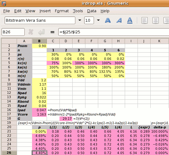
As shown on the right, a spreadsheet can be used to iterate to the answer
of p=4.40%.
The calculation of the die size including straps is on
the next page.
