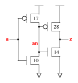
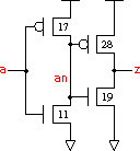
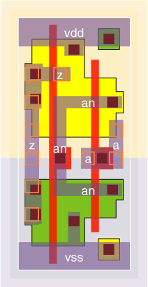
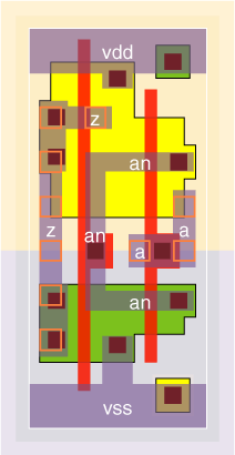
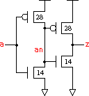
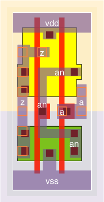
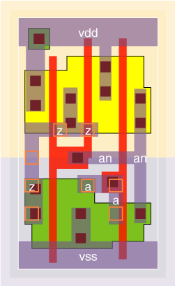
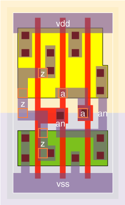
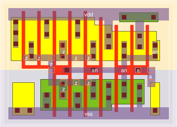
bf1 standard cell family

non-inverting buffer
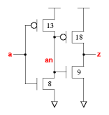
bf1 symbol
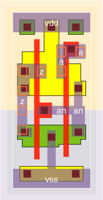
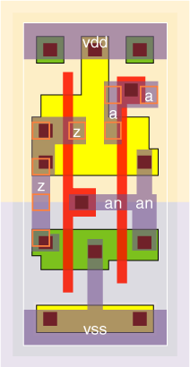
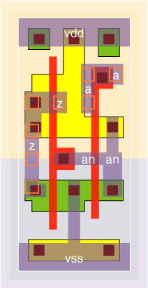
The buffers allow a large load to be driven with a small input capacitance. The selection includes a variety of stage efforts and P/N transistor ratios.
The buffers have an output P/N ratio of 2 except for the v1 version which uses a P/N ratio of 1.5. A P/N ratio of 2 offers good output skew, while 1.5 is close to the fastest speed.
The stage effort of the v0, v1 and v2 cells is designed to optimise speed with typical wireload values. The v4 version provides a minimum input capacitance. The inverters of the v5 version are the same size, so the delay is minimised at the expense of a higher input capacitance.
The v0 and v2 versions are similar, but use different P/N ratios on the first stage. The v2 cells use a first stage P/N ratio of 2. The v0 version tries to optimise the average delay by adjusting the first stage P/N ratio. The FO4 measure shows the delays relative to an iv1v2x2.
The v6 and v8 versions are experimental versions looking at the effect of layout and transistor size variations.
The v0 and v2 stage efforts are 1.3 for the x05; 1.5 for the x1; 1.8 x2; 2.1 x3, 2.3 x4, 2.6 x6, 2.8 x8 and 3.1 for the x12. The stage effort for the v5 buffers is 1.2.
z:a cell width power Generic 0.13um typical timing (ps & ps/fF), pin a.
leakage dynamic tR=PropR+RampR×Load(fF), tF=PropF+RampF×Load(fF)
vsclib013 gates lambda 0.13um nW nW/MHz PinCap PropR RampR PropF RampF
bf1v0x05 1.3  32 1.76  0.40   9.7  2.2f  53  4.94  77  3.83
bf1v5x05 1.3  32 1.76  0.42   9.8  2.3f  58  4.94  70  3.82
bf1v0x1 1.3  32 1.76  0.55  13.1  2.7f  56  3.29  76  2.54
bf1v2x1 1.3  32 1.76  0.55  12.9  2.5f  60  3.29  76  2.54
bf1v4x1 1.3  32 1.76  0.45  11.7  1.6f  59  3.29 106  2.59
bf1v5x1 1.3  32 1.76  0.62  14.8  3.5f  59  3.30  71  2.54
bf1v0x2 1.3  32 1.76  0.80  19.4  3.4f  61  2.12  80  1.65
bf1v1x2 1.3  32 1.76  0.87  21.1  3.5f  61  2.12  80  1.23
bf1v2x2 1.3  32 1.76  0.80  19.4  3.4f  65  2.12  78  1.65
bf1v5x2 1.3  32 1.76  0.97  21.9  5.2f  56  2.12  68  1.64
bf1v6x2 1.3  32 1.76  0.75  18.1  3.2f  66  2.20  79  1.92
bf1v0x3 1.7  40 2.20 1.09  24.9  4.3f  63  1.48  80  1.14
bf1v2x3 1.7  40 2.20 1.07  24.8  4.2f  65  1.48  79  1.14
bf1v0x4 1.7  40 2.20 1.46  32.9  5.2f  64  1.06  83  0.83
bf1v2x4 1.7  40 2.20 1.46  32.9  5.2f  67  1.06  81  0.83
bf1v5x4 2.3  56 3.08 1.94  37.3 10.2f  49  1.06  62  0.82
bf1v8x4 1.7  40 2.20 1.25  30.0  3.0f  85  1.06 103  0.84
bf1v0x6 2.7  64 3.52 2.03  45.0  6.5f  65  0.73  82  0.57
bf1v2x6 2.7  64 3.52 2.02  44.8  6.4f  67  0.73  82  0.57
bf1v0x8 3.0  72 3.96 2.56  56.6  7.8f  66  0.56  84  0.45
bf1v2x8 3.0  72 3.96 2.56  56.5  7.8f  68  0.56  83  0.44
bf1v0x12 4.3 104 5.72 3.83  85.9 10.3f  69  0.36  90  0.28
bf1v0x05
 
Effort
FO4 Log.
a /\
¯_ 1.49
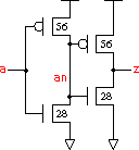
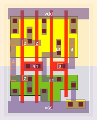
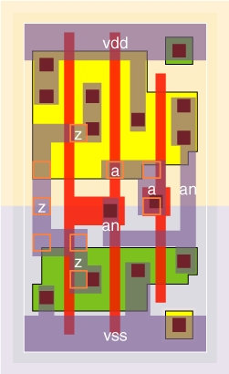
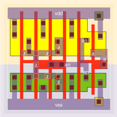
bf1v0x05 schematic bf1v0x05 standard cell layout
bf1v5x05
 
Effort
FO4 Log.
a /\
¯_ 1.50
bf1v5x05 schematic bf1v5x05 standard cell layout
bf1v0x1
 
Effort
FO4 Log.
a /\
¯_ 1.39
bf1v0x1 schematic bf1v0x1 standard cell layout
bf1v2x1
 
Effort
FO4 Log.
a /\
¯_ 1.39
bf1v2x1 schematic bf1v2x1 standard cell layout
bf1v4x1
 
Effort
FO4 Log.
a /\
¯_ 1.45
bf1v4x1 schematic bf1v4x1 standard cell layout
bf1v5x1
 
Effort
FO4 Log.
a /\
¯_ 1.51
bf1v5x1 schematic bf1v5x1 standard cell layout
bf1v0x2
 
Effort
FO4 Log.
a /\
¯_ 1.38
bf1v0x2 schematic bf1v0x2 standard cell layout
bf1v1x2
 
Effort
FO4 Log.
a /\
¯_ 1.36
bf1v1x2 schematic bf1v1x2 standard cell layout
bf1v2x2
 
Effort
FO4 Log.
a /\
¯_ 1.39
bf1v2x2 schematic bf1v2x2 standard cell layout
bf1v5x2
 
Effort
FO4 Log.
a /\
¯_ 1.46
bf1v5x2 schematic bf1v5x2 standard cell layout
bf1v6x2
 
Effort
FO4 Log.
a /\
¯_ 1.41
bf1v6x2 schematic bf1v6x2 standard cell layout
bf1v0x3
 
Effort
FO4 Log.
a /\
¯_ 1.35
bf1v0x3 schematic bf1v0x3 standard cell layout
bf1v2x3
 
Effort
FO4 Log.
a /\
¯_ 1.35
bf1v2x3 schematic bf1v2x3 standard cell layout
bf1v0x4
 
Effort
FO4 Log.
a /\
¯_ 1.33
bf1v0x4 schematic bf1v0x4 standard cell layout
bf1v2x4
 
Effort
FO4 Log.
a /\
¯_ 1.34
bf1v2x4 schematic bf1v2x4 standard cell layout
bf1v5x4
 
Effort
FO4 Log.
a /\
¯_ 1.35
bf1v5x4 schematic bf1v5x4 standard cell layout
bf1v8x4
 
Effort
FO4 Log.
a /\
¯_ 1.50
bf1v8x4 schematic bf1v8x4 standard cell layout
bf1v0x6
 
Effort
FO4 Log.
a /\
¯_ 1.30
bf1v0x6 schematic bf1v0x6 standard cell layout
bf1v2x6
 
Effort
FO4 Log.
a /\
¯_ 1.31
bf1v2x6 schematic bf1v2x6 standard cell layout
bf1v0x8
 
Effort
FO4 Log.
a /\
¯_ 1.31
bf1v0x8 schematic bf1v0x8 standard cell layout
bf1v2x8
 
Effort
FO4 Log.
a /\
¯_ 1.31
bf1v2x8 schematic bf1v2x8 standard cell layout
bf1v0x12
 
Effort
FO4 Log.
a /\
¯_ 1.34
bf1v0x12 schematic bf1v0x12 standard cell layout