nr2 standard cell family

2-I/P NOR gate
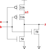
nr2 symbol
nr2 effort graph The fastest speed occurs when the shape factor r=√( KP÷ KN×µ). For a 2-NOR gate, we use KP=15/8; KN=1, and µ=9/4, which gives r=√(135/32)≈2. This value has been used for the v1 version, which are fast with unbalanced output skews. The P/N ratio has been kept as close to 2 as possible for the v0 version in order to give more balanced output skews, even if this is not the fastest configuration.
The effort measured by the fanout=4 method is shown in the graph on the right, which shows that the v1 cells are generally faster than the v0 cells. The variations are caused by the parasitic capacitances.
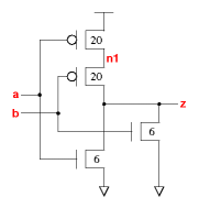
z:(a+b)' cell width power Generic 0.13um typical timing (ps & ps/fF), pin b.
leakage dynamic tR=PropR+RampR×Load(fF), tF=PropF+RampF×Load(fF)
vsclib013 gates lambda 0.13um nW nW/MHz PinCap PropR RampR PropF RampF
nr2v0x05 1.3  32 1.76  0.37   5.0  2.9f  45  5.81  40  3.86
nr2v1x05 1.3  32 1.76  0.34   4.5  2.6f  49  7.75  35  3.36
nr2v0x1 1.3  32 1.76  0.51   6.9  3.9f  44  4.15  41  2.89
nr2v1x1 1.3  32 1.76  0.65   7.8  4.6f  48  4.13  32  1.72
nr2v0x2 2.0  48 2.64  0.97  10.6  7.3f  40  2.15  38  1.55
nr2v1x2 2.3  56 3.08 1.22  13.6  8.8f  45  2.15  31  0.92
nr2v0x3 2.7  64 3.52 1.52  18.2 11.2f  42  1.38  40  0.96
nr2v1x3 2.7  64 3.52 1.89  21.2 13.6f  45  1.38  31  0.60
nr2v0x4 3.3  80 4.40 1.99  22.0 15.2f  40  1.04  38  0.77
nr2v1x4 3.3  80 4.40 2.47  26.6 17.6f  45  1.07  30  0.45
nr2v0x6 5.3 128 7.04 2.98  33.1 22.8f  40  0.69  38  0.52
nr2v1x6 5.3 128 7.04 3.79  41.6 27.2f  45  0.69  31  0.30
nr2v0x8 6.3 152 8.36 3.83  42.6 29.1f  40  0.54  38  0.40
nr2v1x8 6.3 152 8.36 4.68  50.9 33.4f  45  0.56  31  0.24
nr2v0x05
 
Effort
FO4 Log.
a /\ 1.55 1.67
¯_
b /\ 1.41 1.63
¯_
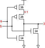
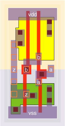
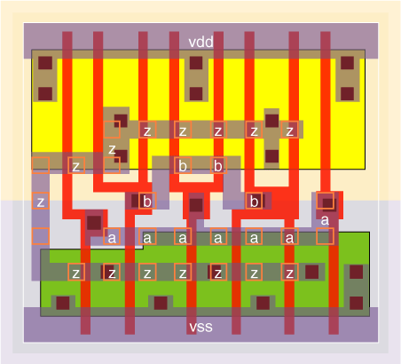
nr2v0x05 schematic nr2v0x05 standard cell layout
nr2v1x05
 
Effort
FO4 Log.
a /\ 1.51 1.65
¯_
b /\ 1.41 1.65
¯_
nr2v1x05 schematic nr2v1x05 standard cell layout
nr2v0x1
 
Effort
FO4 Log.
a /\ 1.53 1.62
¯_
b /\ 1.39 1.58
¯_
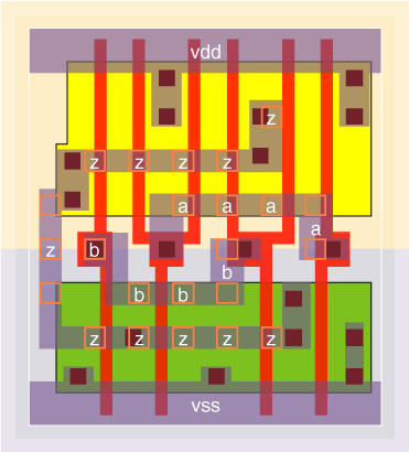
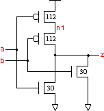
nr2v0x1 schematic nr2v0x1 standard cell layout
nr2v1x1
 
Effort
FO4 Log.
a /\ 1.45 1.60
¯_
b /\ 1.34 1.57
¯_
nr2v1x1 schematic nr2v1x1 standard cell layout
nr2v0x2
 
Effort
FO4 Log.
a /\ 1.51 1.67
¯_
b /\ 1.33 1.58
¯_
nr2v0x2 schematic nr2v0x2 standard cell layout
nr2v1x2
 
Effort
FO4 Log.
a /\ 1.48 1.67
¯_
b /\ 1.32 1.57
¯_
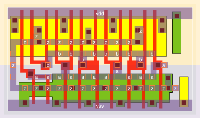
nr2v1x2 schematic nr2v1x2 standard cell layout
nr2v0x3
 
Effort
FO4 Log.
a /\ 1.50 1.61
¯_
b /\ 1.33 1.53
¯_
nr2v0x3 schematic nr2v0x3 standard cell layout
nr2v1x3
 
Effort
FO4 Log.
a /\ 1.44 1.60
¯_
b /\ 1.32 1.57
¯_
nr2v1x3 schematic nr2v1x3 standard cell layout
nr2v0x4
 
Effort
FO4 Log.
a /\ 1.52 1.67
¯_
b /\ 1.35 1.61
¯_
nr2v0x4 schematic nr2v0x4 standard cell layout
nr2v1x4
 
Effort
FO4 Log.
a /\ 1.45 1.63
¯_
b /\ 1.31 1.56
¯_
nr2v1x4 schematic nr2v1x4 standard cell layout
nr2v0x6
 
Effort
FO4 Log.
a /\ 1.52 1.66
¯_
b /\ 1.35 1.60
¯_
nr2v0x6 schematic nr2v0x6 standard cell layout
nr2v1x6
 
Effort
FO4 Log.
a /\ 1.45 1.63
¯_
b /\ 1.32 1.57
¯_
nr2v1x6 schematic nr2v1x6 standard cell layout
nr2v0x8
 
Effort
FO4 Log.
a /\ 1.52 1.66
¯_
b /\ 1.35 1.59
¯_
nr2v0x8 schematic nr2v0x8 standard cell layout
nr2v1x8
 
Effort
FO4 Log.
a /\ 1.45 1.62
¯_
b /\ 1.32 1.56
¯_
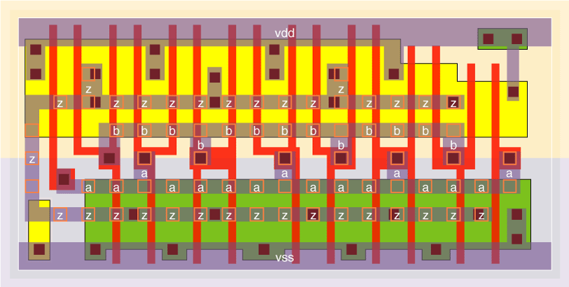
nr2v1x8 schematic nr2v1x8 standard cell layout